Who We Are
Engineering India’s Innovation Frontier, One Product at a Time
Engineering India’s Innovation Frontier, One Product at a Time
Founded with a vision to accelerate innovation from napkin sketch to product launch, Ultimate Design Technology LLP is a legally incorporated, India-based product development firm. We specialize in end-to-end electronics and full-stack software development—seamlessly integrating mechanical, embedded, and digital systems under one roof.
With a multidisciplinary team of engineers, designers, and product strategists, we empower startups, OEMs, and global innovators to turn bold ideas into manufacturable, market-ready devices. Our approach is deeply rooted in Indian ingenuity, agile execution, and a commitment to global-grade quality.
We handle everything from industrial design, PCBA, embedded programming, mobile/web apps, to compliance and packaging.

We handle everything from industrial design, PCBA, embedded programming, mobile/web apps, to compliance and packaging.


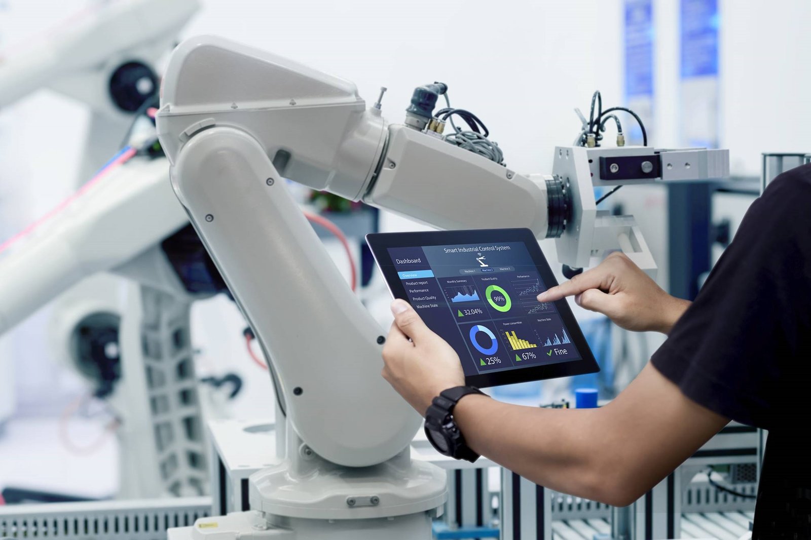
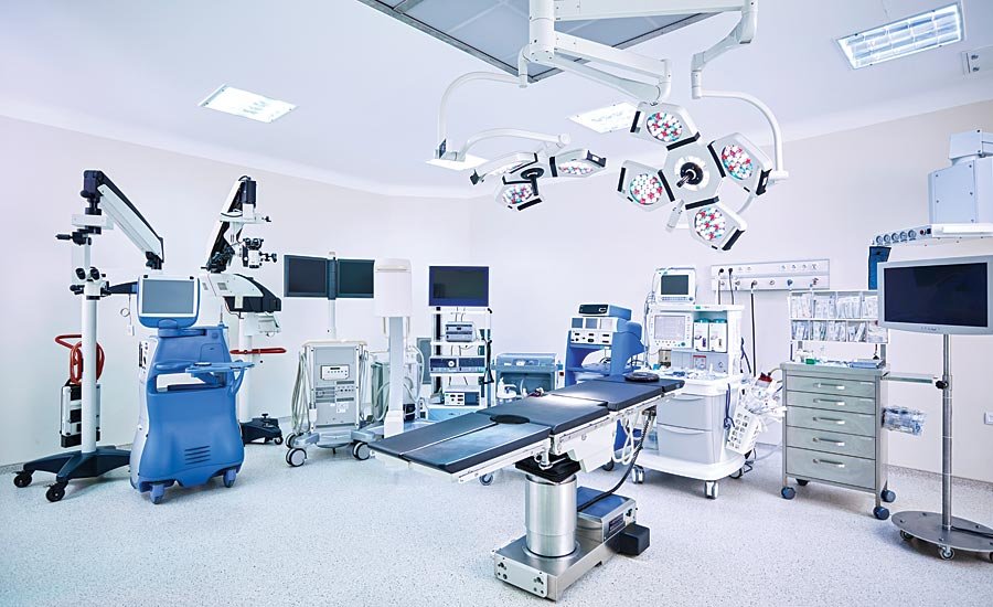
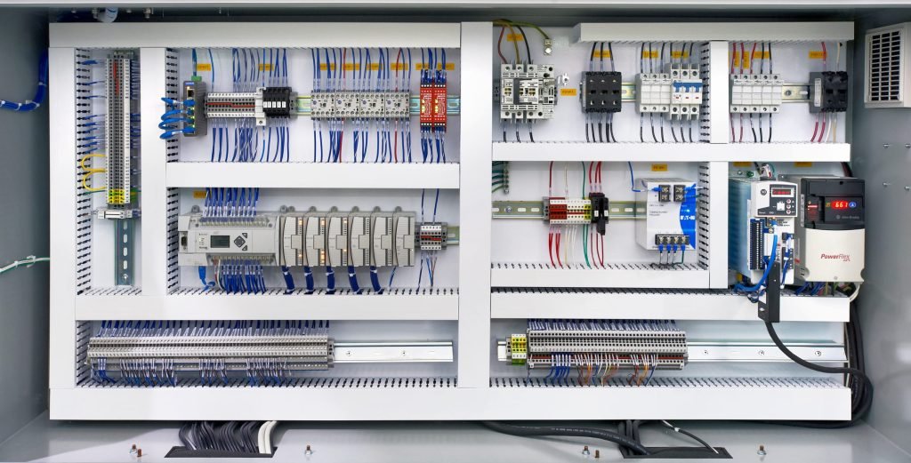
Empowering Innovation Across Every Sector We Touch


Tools That Power Our End-to-End Product Development


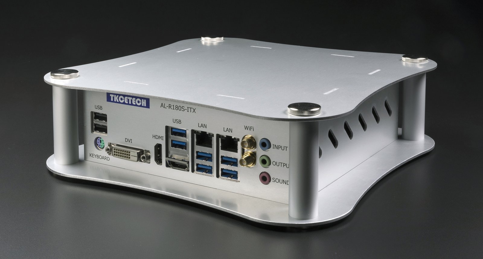
We use industry-leading CAD platforms to create precise mechanical designs and enclosure models that align perfectly with internal electronics — ensuring seamless fit, function, and manufacturability.


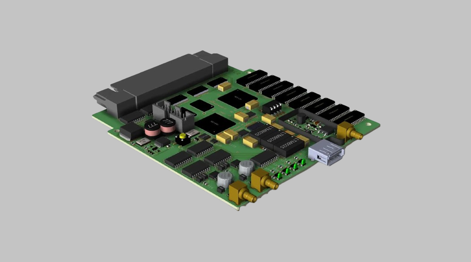
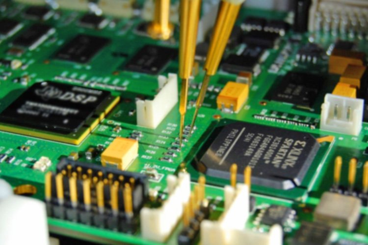
From schematic to Gerber, our team designs robust, production-ready PCBs using advanced tools trusted for both rapid prototyping and high-volume manufacturing.
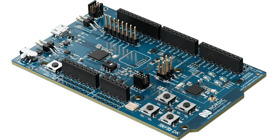
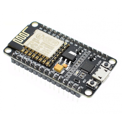
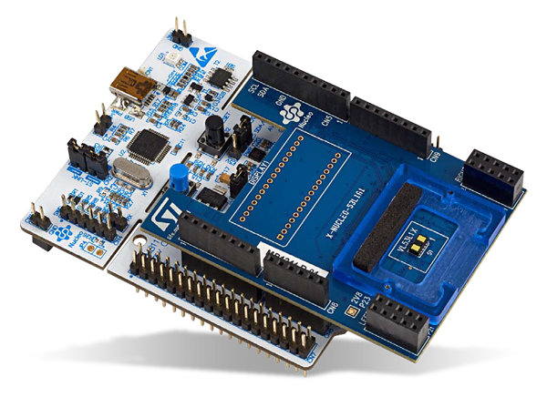
Our firmware is built on proven microcontroller platforms for BLE, Wi-Fi, and edge processing — optimized for performance, stability, and low-power operation across embedded systems.


We develop responsive mobile and web applications that interact seamlessly with hardware products, enabling rich IoT experiences and smart device control from anywhere.


Our cloud integrations power real-time device connectivity, analytics, and remote management — enabling scalable, secure infrastructure for modern connected products.
Built, Tested, and Perfected
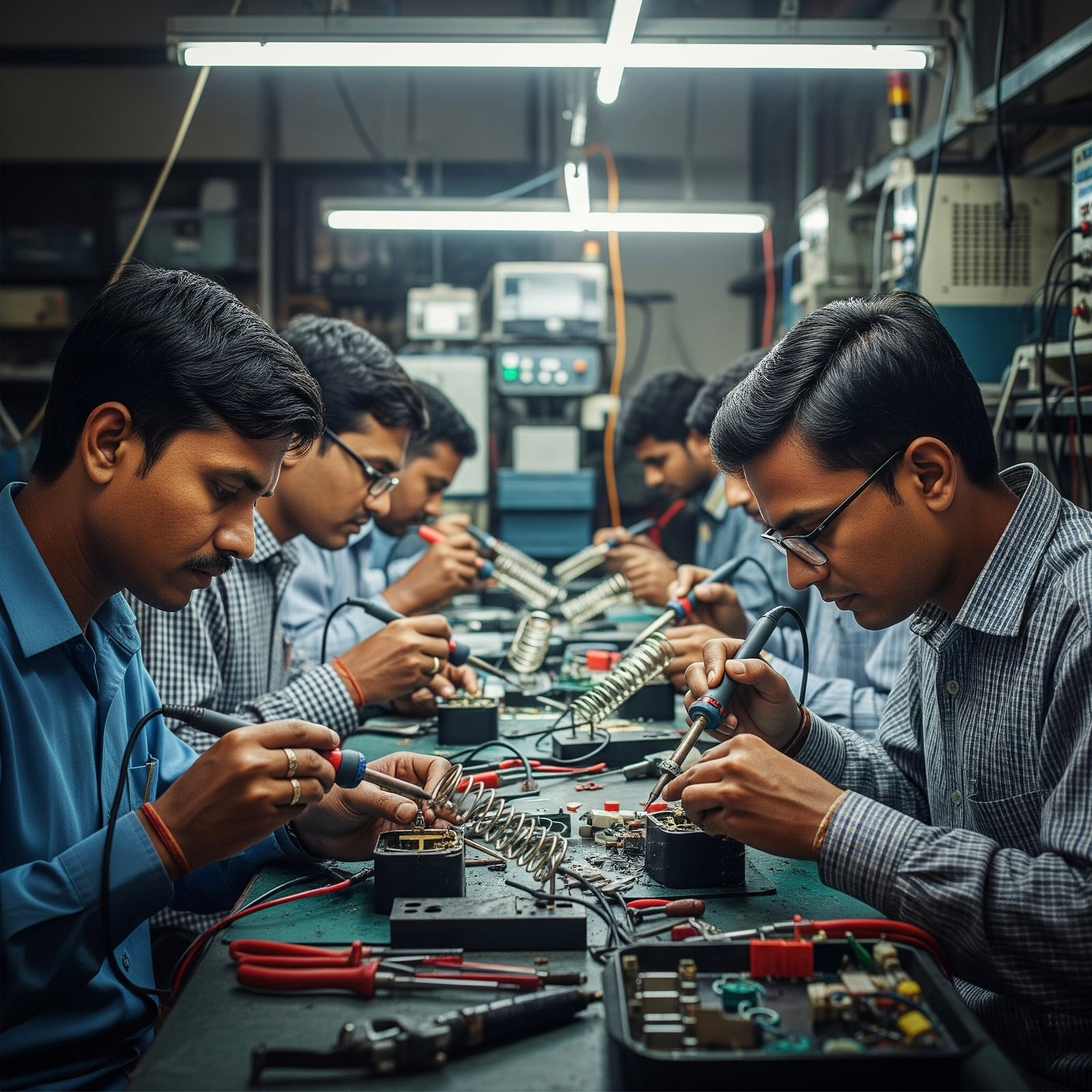
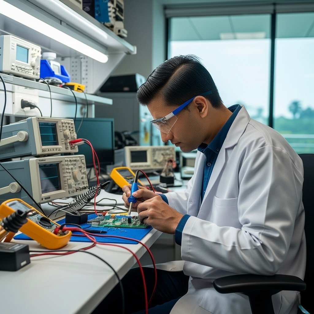
High-precision workstations for manual and reflow soldering of PCBs, supporting both prototyping and small-batch runs.
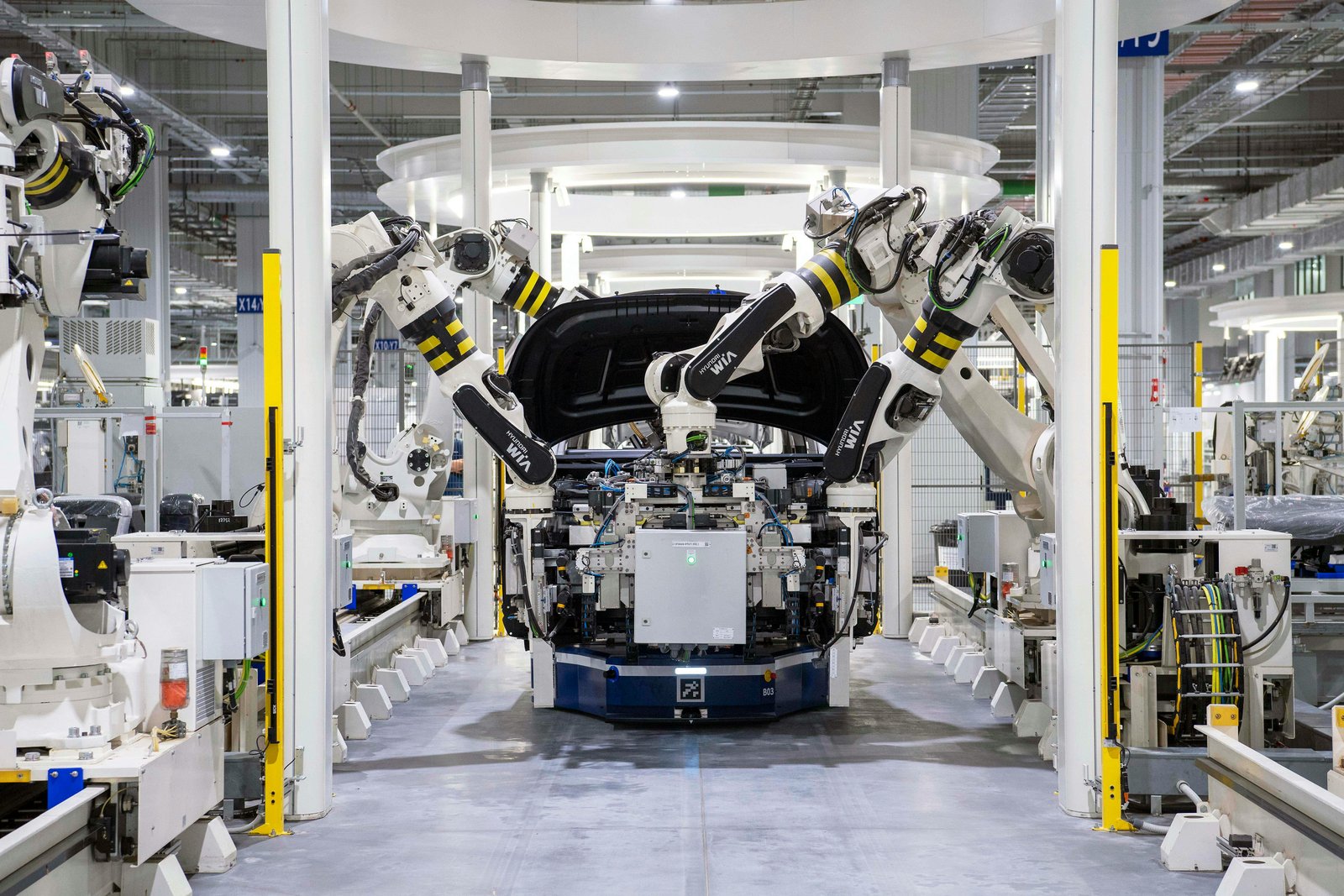
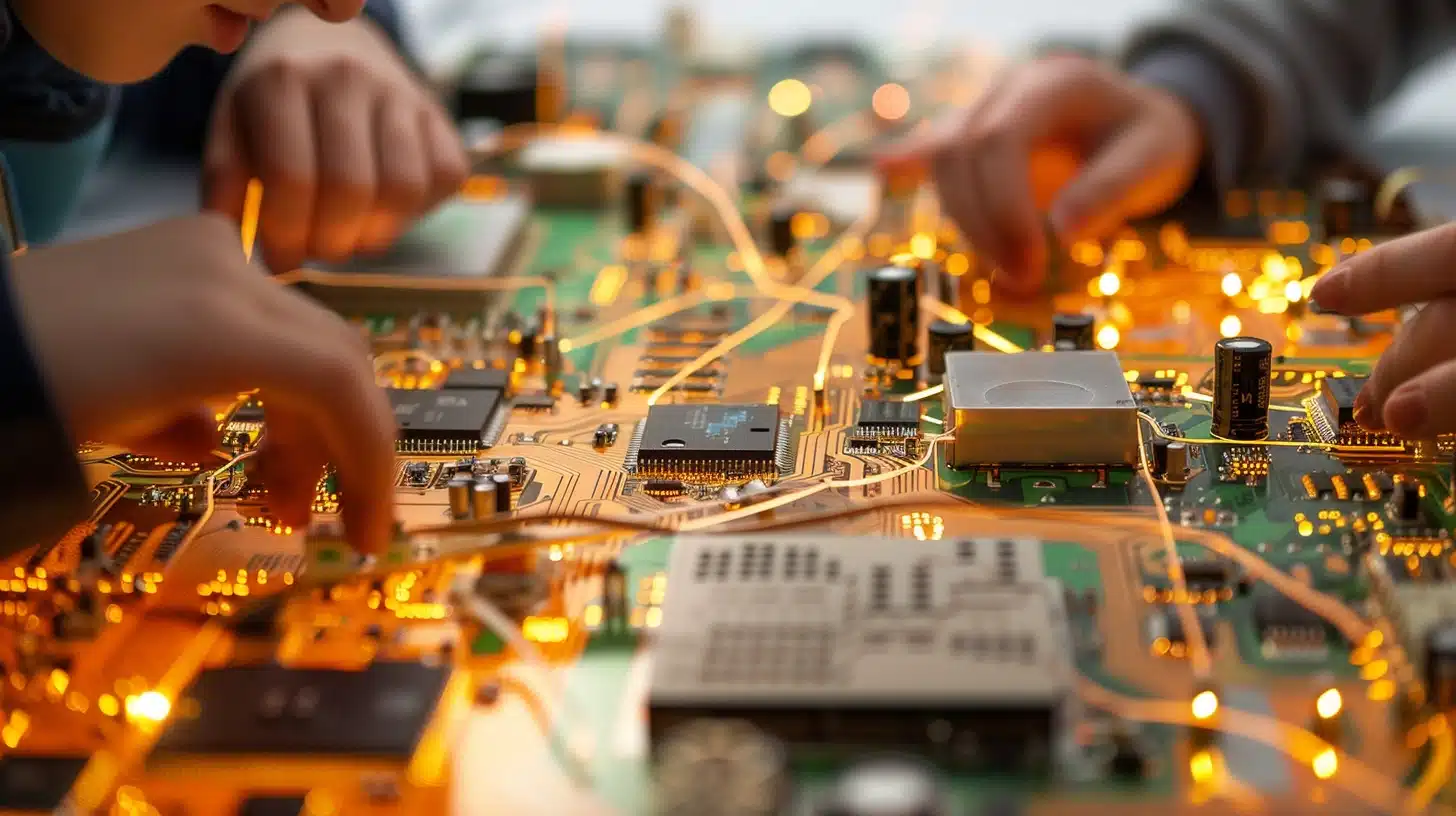
Streamlined setup for rapid component integration, mechanical assembly, and product casing — optimized for agility and scale.
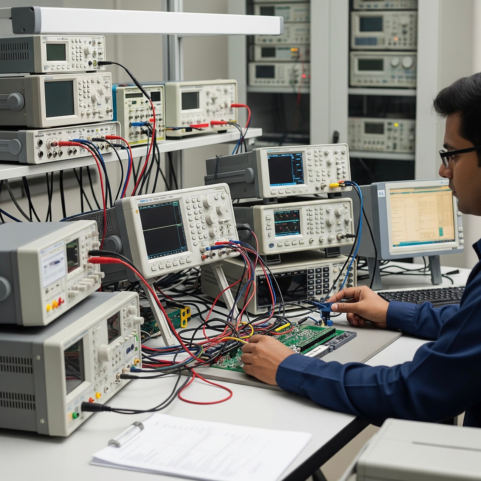
Equipped with oscilloscopes, multimeters, and signal analyzers to validate functionality, performance, and reliability.
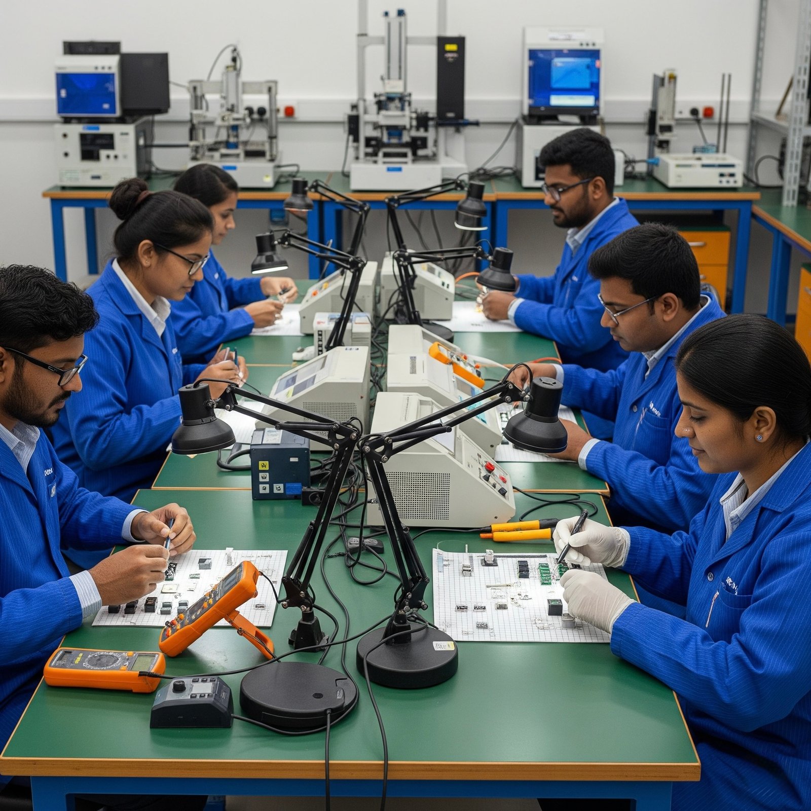
Dedicated zones for iterative design, hardware debugging, and final quality assurance before pilot production.

Controlled environments for fine-pitch components and optical systems, enabling microscopic inspection and dust-free processes.
Localized, Agile, and Built for Precision at Every Step

Discovery

Industrial Design

Prototype

Field Test

Production
Why Indian Engineering Gives You a Global Advantage

One Click Away from Product Innovation